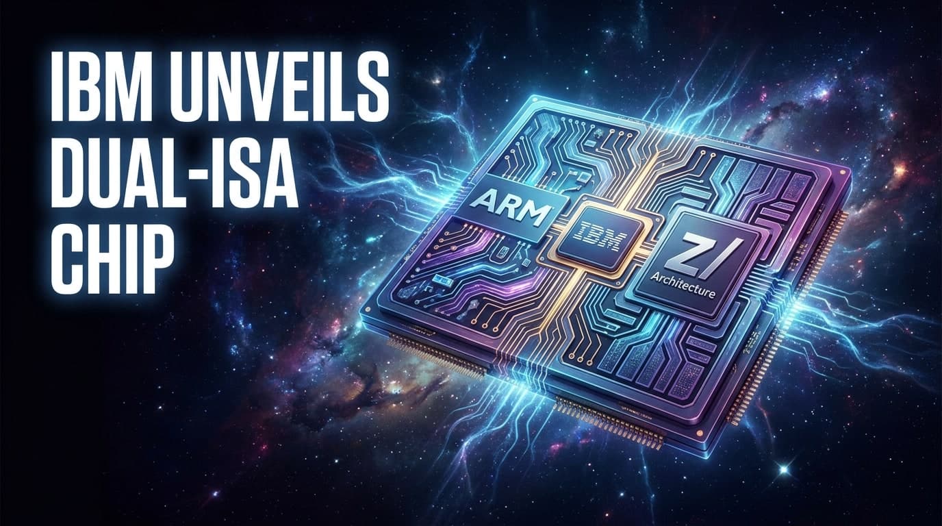
IBM Unveils Dual-ISA Chip Core for ARM and Mainframes
IBM has built a processor core that runs ARM and z/Architecture instructions natively, without any translation software in between. This shift in mainframe chip design could eventually speed up the AI systems that power wallets, wearables, and other connected devices people rely on daily.
What actually happened
The new core sits inside IBM's next-generation mainframe AI processor, built on a 2nm manufacturing process, according to Tom's Hardware. The chip packs 11 cores, and every core runs at a base frequency of 5.7 GHz. IBM calls it the company's first core able to execute two separate instruction set architectures side by side. It skips the translation layer that normally bridges ARM and z/Architecture software. The design lets a single mainframe chip run enterprise z/Architecture programs and ARM-based applications on the same hardware, according to the report. IBM frames the design as part of a broader effort to expand the range of software a single mainframe chip can run natively.
How we got here
Mainframes have used their own proprietary instruction set for decades. That kept them separate from the ARM chips found in phones, edge devices, and much of today's cloud infrastructure. Blending both sets on one core, rather than relying on emulation or extra chips, marks a structural change for IBM. It also fits a wider chip industry trend, shrinking process nodes toward 2nm while asking each chip to handle more types of workloads. Details on how this core compares with IBM's earlier mainframe chips were not part of the current reporting.
Why this matters for you
For everyday wallet users, this chip lives far from any phone or app, but it shapes the infrastructure behind them. Enterprises could run AI and legacy banking systems on one mainframe chip, without slow emulation. That may lower costs for the backend services that process payments, identity checks, and other financial data behind the scenes. For the bonuz ecosystem, faster and more flexible enterprise chips could eventually support quicker AI processing behind wearable and AR features. IBM has not named any consumer or edge product plans.
The bigger question
If one processor core can natively handle two very different instruction sets, does the chip industry still need separate lines for enterprise and AI hardware? Or does merging architectures on a single core become the standard path for future devices, from mainframes to the glasses and wearables people use daily? The answer could shape how future chips, from mainframes to wearable devices, get designed and priced.
What to watch
IBM has not shared a public release date, product name, or launch event for this processor, according to current reporting. Watch for official specifications, benchmark results, and deployment timelines in IBM's next hardware announcement. Comparisons with IBM's earlier mainframe chips should clarify how big this change really is. Bonuz will track official IBM specifications as they arrive.